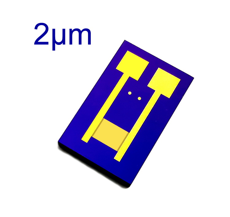
2 micron silicon-based silicon dioxide interdigital gold electrode photoelectric detection sensor chip MEMS high precision
1. The electrode substrate is monocrystalline silicon, and silicon dioxide is grown on the surface of the silicon wafer with a thickness of 300nm; overall dimensions: 5mm*8mm*0.52mm.
2. Line width: 5um, line distance: 2um, finger length: 1.8mm, number of interdigital fingers: 100 (200 fingers).
3. Metal layer structure: Cr/Au, thickness is 30nm, 100nm;
4. Electrode operating temperature range: -150��~500��;
5. Large size, large pad and easy operation;
6. Mainly used in various chemical, physical and medical sensors, with reliable performance and stable quality.
7. Large quantity and preferential price.
We provide various interdigital electrodes. Including different shapes, different sizes, different line widths, different substrates (oxidized
Aluminum ceramics, PI/PET flexible materials, monocrystalline silicon), different processes (thick film process, DPC process, MEMS process).


| Warm tips: Suzhou Beike nano products are only used for scientific research, not for human body,different batches of products have different specifications and performance |
Message
|
|
 |
Scan code concerns WeChat official account
QQCommunication group��1092348845
|
|
| Warm tips: Suzhou Beike nano products are only used for scientific research, not for human body,different batches of products have different specifications and performance.The website pictures are from the Internet. The pictures are for reference only. Please take the real object as the standard. In case of infringement, please contact us to delete them immediately. |