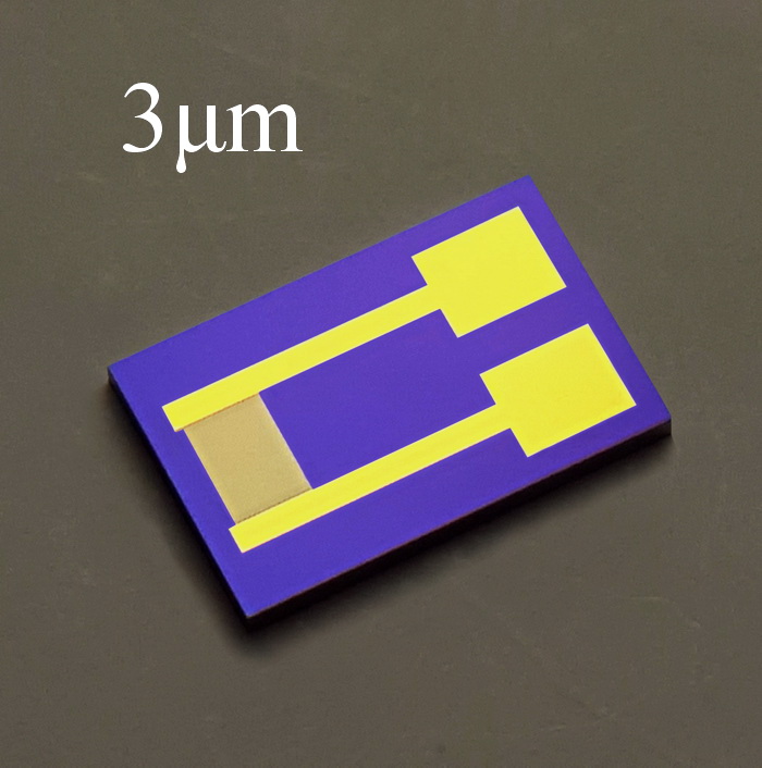
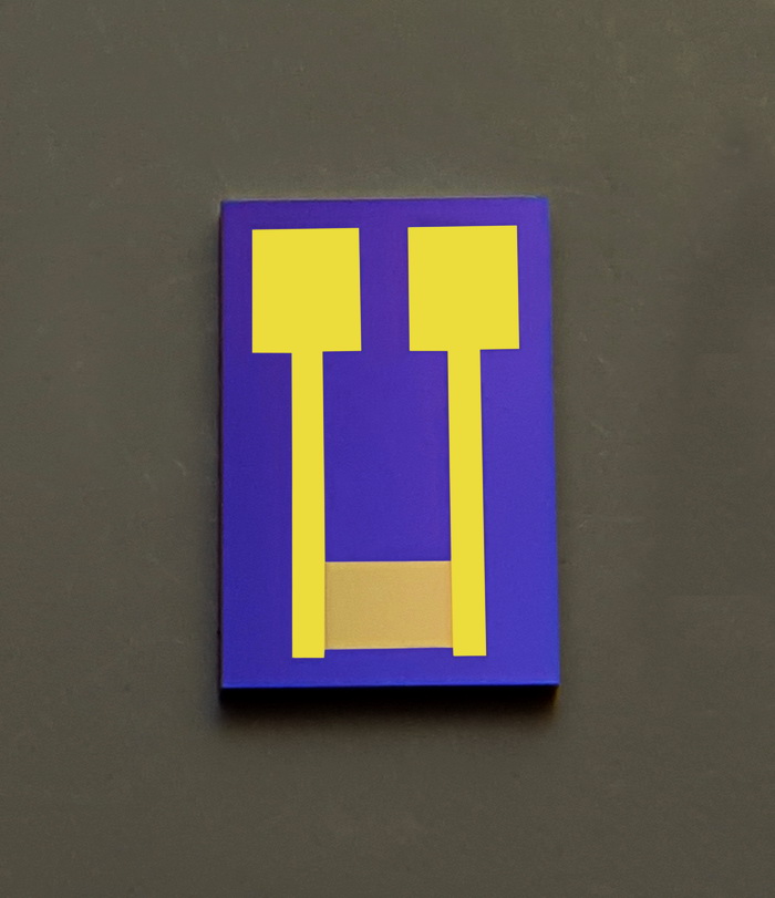
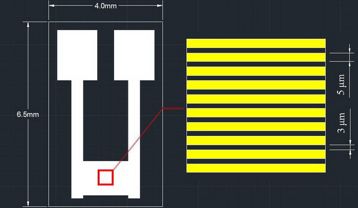
1. Dimensions: 4mm*6.5mm*0.52mm.
2. Line width: 10 u m, line spacing: 10 u m, finger length: 1.6mm, interdigital logarithm: 50 (100 fingers).
3. The electrode substrate is monocrystalline silicon, and silicon dioxide is grown on the surface of the silicon wafer with a thickness of 300nm;
4. Metal layer structure: Ti/Au, thickness is 30nm, 100nm;
5. Electrode operating temperature range: -150��~500��;
6. Mainly used in various chemical, physical and medical sensors, with reliable performance and stable quality.


| Warm tips: Suzhou Beike nano products are only used for scientific research, not for human body,different batches of products have different specifications and performance |
Message
|
|
 |
Scan code concerns WeChat official account
QQCommunication group��1092348845
|
|
| Warm tips: Suzhou Beike nano products are only used for scientific research, not for human body,different batches of products have different specifications and performance.The website pictures are from the Internet. The pictures are for reference only. Please take the real object as the standard. In case of infringement, please contact us to delete them immediately. |


